Robotic Sensor Module Design
Artificial Fingertip with Tactile Sensing for Humanoid Robots
I developed a high-density tactile fingertip capable of sensing pressure and vibration in a compact form factor. It was designed for humanoid robotic hands and developed as part of my research in tactile sensing.
High-density tactile sensing for humanoids and prosthetics
This project focuses on the design and development of a high-density tactile fingertip module intended for humanoid robot and prosthetic hand applications. The module measures pressure on its surface through 22 individual pressure sensors distributed across the fingertip area. It is built with Flexible Printed Circuit Board (Flex-PCB) technology.
An origami technique folds a flat, paper-like flexible tactile sensing module into a three-dimensional shape that mimics the form of a human fingertip. Sensor data acquisition is handled by an onboard 32-bit, low-power microcontroller, and the module communicates over the SPI protocol.
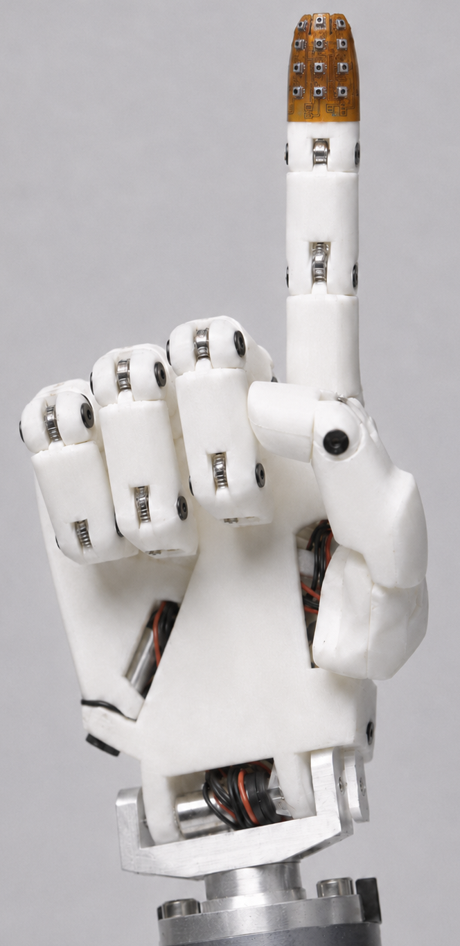
The development of this module presented a number of challenges, particularly in mechanical design and electronics. Before this project I had limited experience with mechanical Computer-Aided Design (CAD). I had to learn how to design both mechanical structures and electronic schematics, and manage the manufacturing and integration processes.
Despite these challenges, a functional prototype was developed. While the current version is not yet optimised for production, it is capable of capturing tactile data. The dimensions of the fingertip closely match those of a typical human fingertip, enabling applications in humanoid robots and prosthetic systems.
CAD model
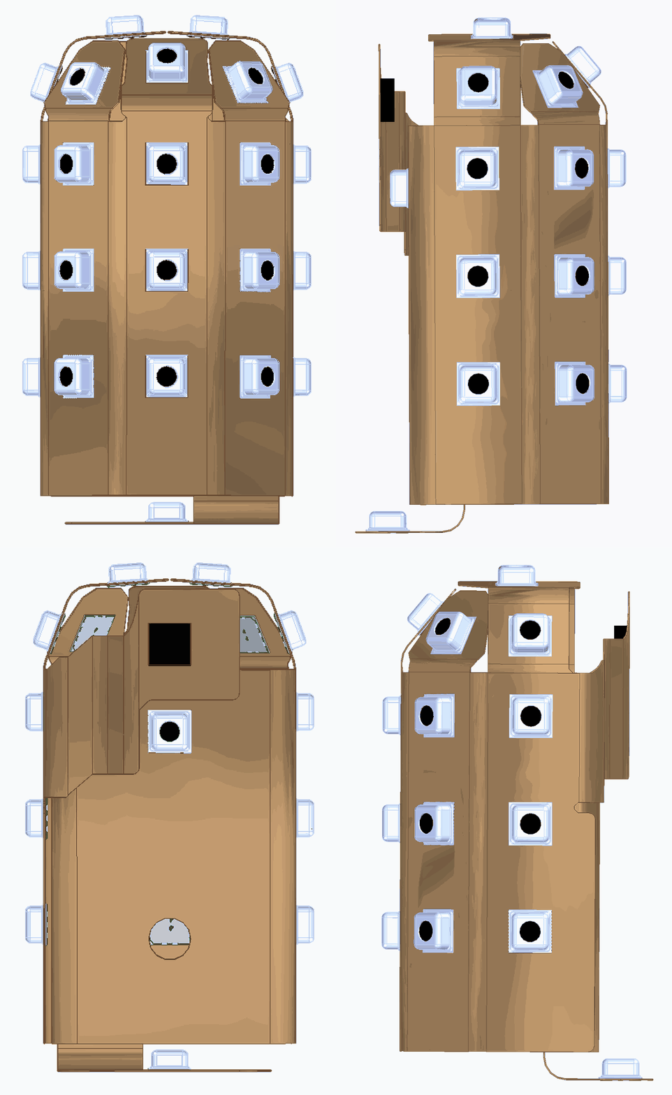
The model was created in Siemens Solid Edge. The sheet metal environment was used to design the foldable flexible-PCB geometry, while the part environment was used to integrate additional components such as the pressure sensors and the onboard microcontroller.
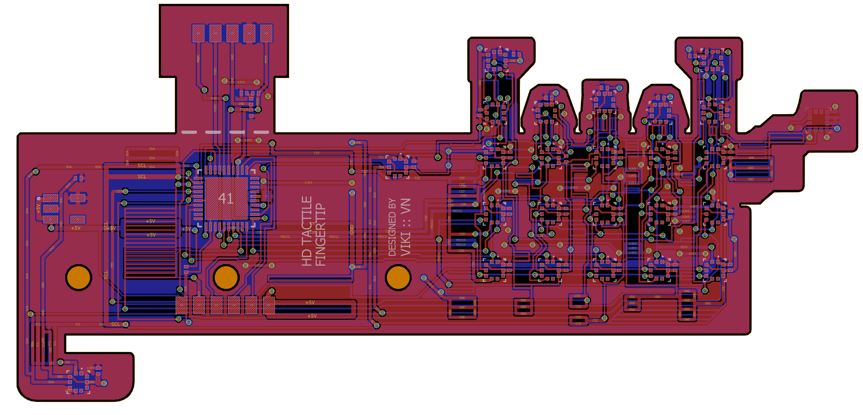
Board layout
The schematics and board layout were designed in Autodesk Eagle. It was a challenging task, as a large number of vias had to be managed within a very small area. The layout includes approximately 218 vias on a two-layer flexible PCB of around 32 mm × 74 mm.
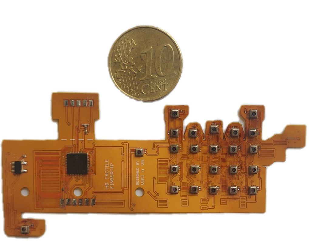
Fully populated module
The module is manufactured on a 2-layer flexible PCB with a thickness of 0.11 mm. After fabrication, surface-mount technology (SMT) is used to populate the electronic components. Figure 3 shows the populated flexible PCB placed next to a 10-cent coin, highlighting the size and the complexity of the design.
Origami
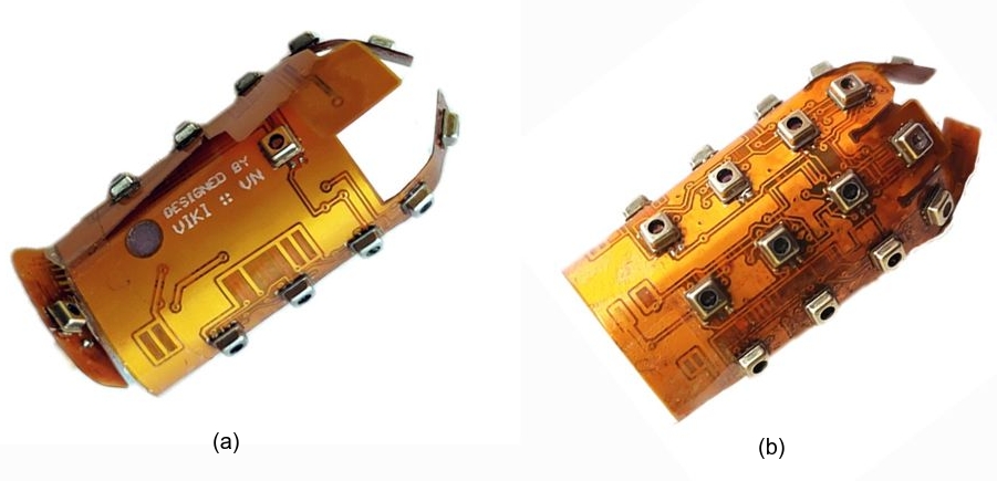
Origami, the traditional Japanese art of folding paper, is applied here to turn the flat flexible module into a 3D shape resembling a fingertip. I do not have much expertise in origami, so I used a simplified version of the technique. Figure 4 shows the folded fingertip from the top (4a) and bottom (4b). The bottom view represents the fleshy part of the fingertip.
Mounted on an open-source InMoov robotic hand
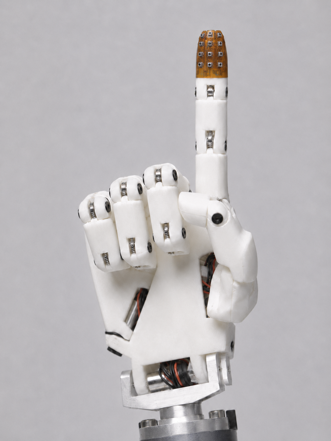
This demonstration is for illustration only. The silicone surface molding and supporting structure are still in progress. At this stage, only the electronics and basic sensor sampling have been tested successfully.
Open source
Parts of this project have been open-sourced, including the tactile controller module and the initial evaluation version of the flexible tactile sensor module with two sensors.
- Tactile Controller Module: https://github.com/neoviki/tactilectr
- Flexible Tactile Sensor with Dual Sensors: https://github.com/neoviki/dualtac
Flexible tactile sensor with dual sensors
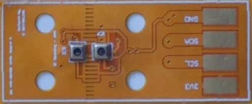
Figure 6 shows the flexible dual-sensor module developed to evaluate hysteresis behaviour in MEMS barometric pressure sensors before continuing with the fingertip-shaped sensor. After obtaining satisfactory results, with minimal or no significant hysteresis, the fingertip sensor with 22 barometric sensors was developed, as shown in Figures 3 and 5.
The dual-sensor module is mounted on a triangular prism-shaped base, with a silicone surface formed above the sensors to mimic the behaviour of human skin. More details about the image, CAD model, sensor data and documentation will be published soon. The EDA design files, including schematics and board layout, are already open-sourced: https://github.com/neoviki/dualtac
Future work
Further development is planned, including data collection, sensor evaluation and communication firmware optimisation. Future updates may include:
- Detailed experimental results
- Sensor performance analysis
- Sampling-frequency and spatial-resolution evaluation
- Additional schematics, data and documentation
These materials have not been published because the project is currently paused while I focus on other work. Once development resumes and the results and documentation reach a satisfactory level, I plan to make them available.